- 您现在的位置:买卖IC网 > Sheet目录2001 > ISL12023IVZ (Intersil)IC RTC/CLDR TEMP SNSR 14-TSSOP
ISL12023
2
FN6682.3
December 6, 2011
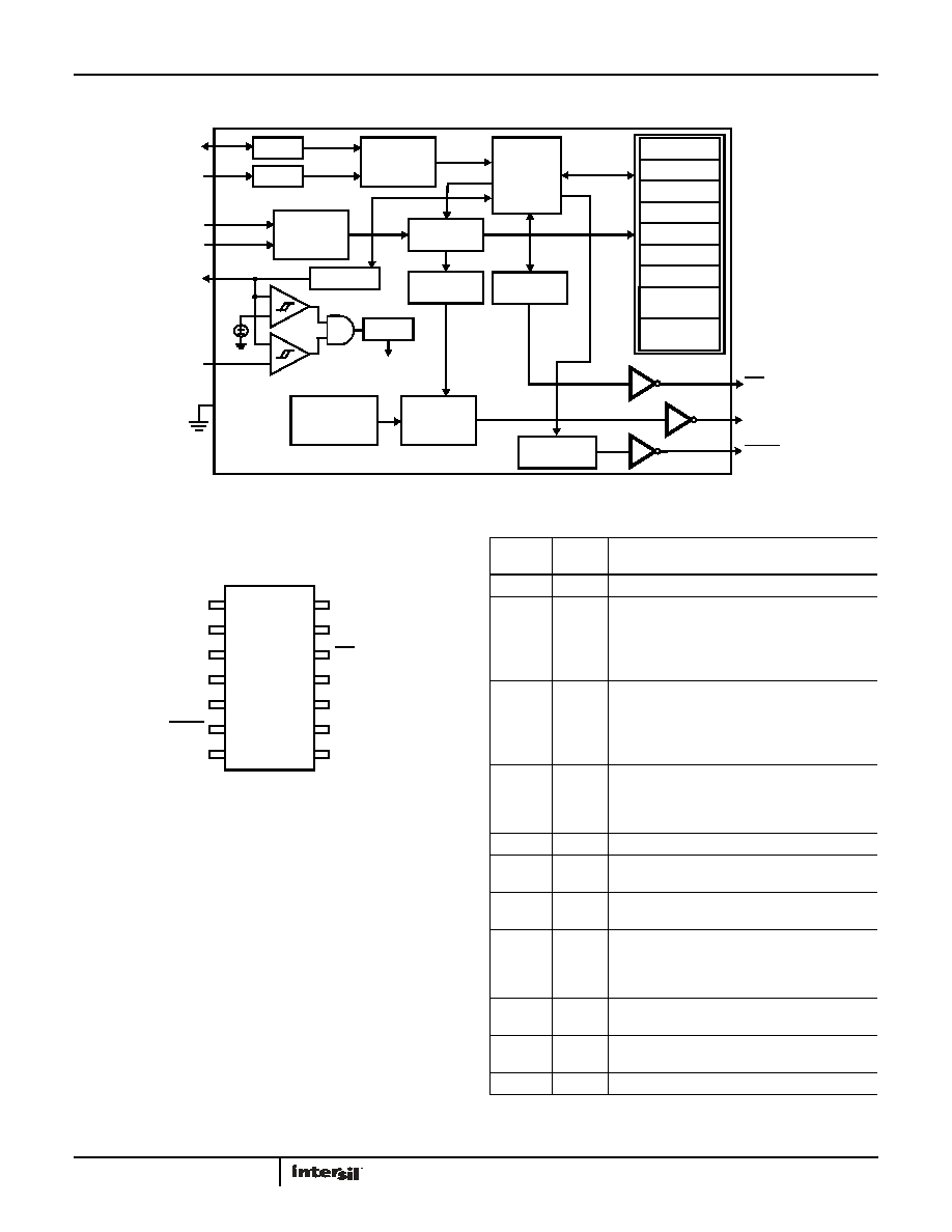
Block Diagram
Pin Configuration
ISL12023
(14 LD TSSOP)
TOP VIEW
GND
I2C
INTERFACE
CONTROL
LOGIC
ALARM
FREQUENCY
OUT
RTC
DIVIDER
SDA
BUFFER
CRYSTAL
OSCILLATOR
POR
SWITCH
SCL
BUFFER
SDA
SCL
X1
X2
VDD
VBAT
INTERNAL
SUPPLY
VTRIP
SECONDS
MINUTES
HOURS
DAY OF WEEK
DATE
MONTH
YEAR
USER
SRAM
CONTROL
REGISTERS
IRQ
FOUT
BROWNOUT
LVRST
ALARM
TEMPERATURE
SENSOR
FREQUENCY
CONTROL
VDD
IRQ
SCL
SDA
X1
X2
VBAT
2
3
4
5
13
12
11
GND
FOUT
LVRST
NC
1
6
7
8
9
10
14
Pin Descriptions
PIN
NUMBER SYMBOL
DESCRIPTION
1, 7, 8, 14
NC
No connect. Do not connect.
2X1
Crystal Input. The X1 pin is the input of an
inverting amplifier and is intended to be
connected to one pin of an external 32.768kHz
quartz crystal. X1 can also be driven directly from a
32.768kHz source.
3X2
Crystal Output. The X2 pin is the output of an
inverting amplifier and is intended to be
connected to one pin of an external 32.768kHz
quartz crystal. X2 should be left open when X1 is
driven from external source.
4VBAT
Backup Supply. This input provides a backup
supply voltage to the device. VBAT supplies power
to the device in the event that the VDD supply
fails. This pin should be tied to ground if not used.
5GND
Ground.
6LVRST
Low Voltage Reset pin for VCC Brownout Mode.
Open drain configuration
9FOUT
Frequency Output. Frequency selectable through
Control Register. Open drain configuration.
10
SDA
Serial Data. SDA is a bi-directional pin used to
transfer serial data into and out of the device. It
has an open drain output and may be wire OR’ed
with other open drain or open collector outputs.
11
SCL
Serial Clock. The SCL input is used to clock all
serial data into and out of the device.
12
IRQ
Interrupt Output. Provides active low interrupt
signal. Open drain configuration.
13
VDD
Power Supply.
发布紧急采购,3分钟左右您将得到回复。
相关PDF资料
ISL12024IRTCZ
IC RTC/CALENDER 64BIT 8-TDFN
ISL12024IVZ
IC RTC/CALENDAR EEPROM 8-TSSOP
ISL12025IVZ
IC RTC/CALENDAR EEPROM 8-TSSOP
ISL12026IBZ-T7A
IC RTC/CALENDAR EEPROM 8SOIC
ISL12027IV27AZ
IC RTC/CALENDAR EEPROM 8-TSSOP
ISL12028IVZ
IC RTC/CALENDAR EEPROM 14-TSSOP
ISL12029IVZ
IC RTC/CALENDAR EEPROM 14-TSSOP
ISL12030IBZ
IC RTC/CALENDAR EEPROM 8-SOIC
相关代理商/技术参数
ISL12023IVZ-T
功能描述:实时时钟 REAL TIME CLK/CLNDR W/TEMP COM 14 L RoHS:否 制造商:Microchip Technology 功能:Clock, Calendar. Alarm RTC 总线接口:I2C 日期格式:DW:DM:M:Y 时间格式:HH:MM:SS RTC 存储容量:64 B 电源电压-最大:5.5 V 电源电压-最小:1.8 V 最大工作温度:+ 85 C 最小工作温度: 安装风格:Through Hole 封装 / 箱体:PDIP-8 封装:Tube
ISL12024
制造商:INTERSIL 制造商全称:Intersil Corporation 功能描述:Real-Time Clock/Calendar with Embedded Unique ID
ISL12024IBZ
功能描述:实时时钟 REAL TIME CLK/CLNDR W/EEPROM IN 8LD RoHS:否 制造商:Microchip Technology 功能:Clock, Calendar. Alarm RTC 总线接口:I2C 日期格式:DW:DM:M:Y 时间格式:HH:MM:SS RTC 存储容量:64 B 电源电压-最大:5.5 V 电源电压-最小:1.8 V 最大工作温度:+ 85 C 最小工作温度: 安装风格:Through Hole 封装 / 箱体:PDIP-8 封装:Tube
ISL12024IBZ-T
功能描述:实时时钟 REAL TIME CLK/CLNDR W/EEPROM IN 8LD RoHS:否 制造商:Microchip Technology 功能:Clock, Calendar. Alarm RTC 总线接口:I2C 日期格式:DW:DM:M:Y 时间格式:HH:MM:SS RTC 存储容量:64 B 电源电压-最大:5.5 V 电源电压-最小:1.8 V 最大工作温度:+ 85 C 最小工作温度: 安装风格:Through Hole 封装 / 箱体:PDIP-8 封装:Tube
ISL12024IRTCZ
功能描述:实时时钟 RTC OUTPUT PROGRAM TO 32KHZ W/EEPROM 8 RoHS:否 制造商:Microchip Technology 功能:Clock, Calendar. Alarm RTC 总线接口:I2C 日期格式:DW:DM:M:Y 时间格式:HH:MM:SS RTC 存储容量:64 B 电源电压-最大:5.5 V 电源电压-最小:1.8 V 最大工作温度:+ 85 C 最小工作温度: 安装风格:Through Hole 封装 / 箱体:PDIP-8 封装:Tube
ISL12024IRTCZ-T
功能描述:实时时钟 RTC OUTPUT PROGRAM TO 32KHZ W/EEPROM 8 RoHS:否 制造商:Microchip Technology 功能:Clock, Calendar. Alarm RTC 总线接口:I2C 日期格式:DW:DM:M:Y 时间格式:HH:MM:SS RTC 存储容量:64 B 电源电压-最大:5.5 V 电源电压-最小:1.8 V 最大工作温度:+ 85 C 最小工作温度: 安装风格:Through Hole 封装 / 箱体:PDIP-8 封装:Tube
ISL12024IVZ
功能描述:实时时钟 REAL TIME CLK/CLNDR W/EEPROM IN 8LD RoHS:否 制造商:Microchip Technology 功能:Clock, Calendar. Alarm RTC 总线接口:I2C 日期格式:DW:DM:M:Y 时间格式:HH:MM:SS RTC 存储容量:64 B 电源电压-最大:5.5 V 电源电压-最小:1.8 V 最大工作温度:+ 85 C 最小工作温度: 安装风格:Through Hole 封装 / 箱体:PDIP-8 封装:Tube
ISL12024IVZ-T
功能描述:实时时钟 REAL TIME CLK/CLNDR W/EEPROM IN 8LD RoHS:否 制造商:Microchip Technology 功能:Clock, Calendar. Alarm RTC 总线接口:I2C 日期格式:DW:DM:M:Y 时间格式:HH:MM:SS RTC 存储容量:64 B 电源电压-最大:5.5 V 电源电压-最小:1.8 V 最大工作温度:+ 85 C 最小工作温度: 安装风格:Through Hole 封装 / 箱体:PDIP-8 封装:Tube